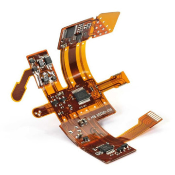
How to bend the PCB?
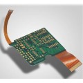
The advanced bent PCB is a multilayer composite wiring board, which laminates a printed wiring board (PWB) and a flexible PCB (FPC) in a multilayer structure. PWB and FPC have copper plated through holes to connect to each other. The circuit board is most suitable for use in small and light equipment.
Features
(1) The new models with the following specifications can be used as the best solution for mobile phones.
·Minimum base thickness: 0.3mm (4 layers), 0.39mm (6 layers)
·Minimum line width/interval: 0.075mm/0.075mm
·Flexibility of single-sided or double-sided flexible PCB (FPC) (as a folding sheet): radius of 3mm, 180° folding, can be folded more than 200,000 times.
(2) It can be connected without contact and at a small pitch, and the equipment can be assembled very compactly in a three-dimensional space.
(3) In the multi-layer (3-8 layers) part, plated through holes are used to realize the connection between the board and the board, thus greatly enhancing the reliability.
(4) The ease of assembly is equivalent to that of a normal printed wiring board.
(5)
A "chip on hole" (chip on hole) specification is available, so that a "blind via hole" (Blind via Holes) can be used as a chip pad.

Overall specifications
Type Foldable type Flying line type
Minimum thickness of substrate*1 0.54mm [4 layers], 0.61mm [6 layers], 0.9mm [8 layers]
Minimum line width/spacing 0.1/0.1mm
Minimum through hole diameter φ0.2mm
The smallest through hole area diameter (through hole) [Outer layer] φ0.5mm,
[Inner layer] φ0.5mm [Outer layer] φ0.5mm,
[Inner layer] φ0.65mm
The smallest through hole area diameter (blind through hole) [Outer layer] φ0.5mm, [Inner layer] φ0.5mm
Minimum diameter of through hole area (built-in through hole) [Inner layer] φ0.5mm
Welding strength Multi-layer: liquid optical solder mask, FPC: film coating
Surface finishing, thermal resistance pre-coated flux, nickel-gold coating, (nickel-gold coating for flying leads)
Safety standard (UL certification) (94V-0)
The structure of advanced bending PCB (6 layers as an example)
Flexible composite multilayer PCB (flexible and robust specifications)
The advanced bent PCB is a multilayer composite wiring board, which laminates a printed wiring board (PWB) and a flexible PCB (FPC) in a multilayer structure. PWB and FPC have copper plated through holes to connect to each other. The circuit board is most suitable for use in small and light equipment.
Features
(1) Multiple pressed layers are internally connected with a flexible PCB (FPC), thus improving the reliability of the connection between the multilayer circuit boards, and reducing the space occupied by the connection and the weight of the joint.
(2) Achieved a narrow interval (0.5mm) of CSP and bare chip mounting, thereby achieving ultra-high-density mounting and making the device more compact and exquisite.
(3) Realization of "internal connection and through-hole connection" and structural lamination, so an ultra-high-density wiring design can be obtained.
(The design provides more free space to make the product smaller and thinner.)
Overall specifications
Type F1 (5th to 8th floors)
Number of layers Hard core layer 1 per side
Floor
Core layer structure 3~6 layers (polyimide, FR-4)
Minimum board thickness 0.8mm (6 layers), 0.87mm (8 layers)
Through hole diameter, round hole diameter Conformal through hole φ0.15mm/φ0.35mm
Stacked through holes ー
Recessed built-in through hole available
Built-in through hole diameter φ0.2mm
Minimum line width/spacing *2 0.09mm/0.09mm
CSP can be installed pitch 0.8mm
Safety standard 94V-0 (waiting for UL certification)
Composite multilayer PCB
Composite multi-layer PCBs can be installed with 0.5mm pitch CSPs, thus reducing the size and thickness of PCBs, enabling high-density mounting design.
Features
(1) Small pitch (0.5mm) CSP ICs and bare chips can be installed in ultra-high density.
(2) Recessed through holes and stacked through structures can realize ultra-fine wiring design.
Overall specifications
Type R1 (4~10 floors)
R2 (6-10 floors)
Number of layers Hard core layer 1 per side
Layer Hard core layer 2 per side
Floor
Core layer structure 2-8 layers (FR-4, FR-5) 2-6 layers (FR-4, FR-5)
The minimum thickness of the board is 0.48mm, (6 layers)
0.6mm, (8 layers) 0.56mm, (6 layers)
0.62mm, (8 layers)
Through hole diameter, round hole diameter Conformal through hole φ0.15mm/φ0.35mm φ0.13mm/φ0.275mm
Laminated through hole ー φ0.15mm/φ0.35mm
Recessed built-in through hole available
Built-in through hole diameter φ0.2mm
Minimum line width/spacing *2 0.09mm/0.09mm 0.075mm/0.075mm
CSP can install pitch 0.8mm 0.5mm
Safety standard (UL certification) 94V-0
Solid PCB
Sharp's rugged PCB can maintain continuous good performance under long-term and harsh conditions, and is known for its excellent reliability, which can meet the various needs of users.
Features
(1) Comply with various specifications, such as SMT/COB/fine mode/multilayer PCB.
(2) From CAD design to circuit board completion, all operations are performed under a fully streamlined command monitoring system.
(3) Flexible PCB and rugged PCB can be combined into Rigid-Flex Board.
Overall specifications
parameter
Overall specifications
Design pattern width
4 floors 6 floors 8 floors
Minimum total thickness 0.35mm 0.45mm 0.6mm
Design pattern width: inner layer: 0.1mm, outer layer: 0.1mm, (partial: 0.075mm)
Design pattern spacing Inner layer: 0.1mm, Outer layer: 0.1mm
Types of through holes Whole through hole, BVH (chip on hole), IVH
Through hole area diameter φ0.2mm (finished)
Finishing processing (surface) thermal resistance pre-coating flux, nickel-gold coating, tin leveling agent
series
Multilayer PCB Double-sided PCB/Others
●Micro-hole PCB ●Low heat dissipation rate ●Micro-hole PCB
●Chip-on-hole PCB
(Chip can be installed)
●Low inductance PCB ●Anti-leakage PCB
●Halogen free
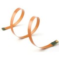
Flexible PCB
Flexible PCB is designed to improve space utilization and product design flexibility, which can meet the needs of smaller
And higher density HDI PCB mounting design needs. It also helps reduce assembly processes and enhance reliability.
Features
(1) High-density mounting circuits, SMT and other most suitable flexible PCBs can be provided.
(2) High-precision type and other electronic connectors installation types for COF with flip chip mounting and circuit bonding capabilities can be provided.
Standard
Number of layers single side
Double-sided through hole
Backing material Polyimide film, adhesive-free polyimide
Design pattern width 0.02 mm (MIN.) 0.05 mm (MIN.)
Design pattern spacing 0.04 mm (MIN.) 0.05 mm (MIN.)
Through hole/land diameter - φ0.1 mm/φ0.3 mm (MIN.)
Covering layer Polyimide film, thermal insulation coating, liquid solder mask
★Series
Multilayer flexible PCB Double-sided flexible PCB
Single layer flexible PCB
Rigid bending PCB
Single-sided high-precision flexible PCB Double-sided high-precision flexible PCB
※other series
Bonded nickel gold coating
Highly flexible type (bending ability)
High density SMT
Contact us if you need more details on Flex Pcb Coverlay. We are ready to answer your questions on packaging, logistics, certification or any other aspects about Flex Pcb Cable、Flex Pcb Electronique. If these products fail to match your need, please contact us and we would like to provide relevant information. Product Categories : Rigid-Flex Board > Flexible Pcb